

The WFPC2 CCDs are thick, front-side illuminated devices, with a format of 800x800, 15x15µm multi-pinned phase (MPP). MPP allows CCD exposure with the total inversion of all phases. The Si-SiO2 interface, at the surface of the CCD, is pinned at the substrate potential, directing signal charge away from the Si-SiO2 interface states towards the buried n-channel. Figure 4.1 shows a schematic which illustrates the principle of MPP (modified from Janesick, et al. 1989). The front-side Si-SiO2 interface significantly affects the performance of CCDs, so MPP operation yields many practical benefits including reduced dark noise, better charge transfer efficiency (CTE), rapid removal of residual images, excellent pixel-to-pixel uniformity, and improved radiation hardness. MPP technology has been demonstrated and characterized in both Loral (Janesick, et al., 1989) and Tektronix devices (Woodgate, et al., 1989). The CCD sensors for WFPC2 were made by Loral in 1991 and processed and packaged for flight at JPL.
Figure 4.1: MPP Operating Principle. A schematic showing the ideal potential profile through a frontside illuminated CCD whose front surface is inverted with multi-pinned phase (MPP). The CCD consists of a polysilicon gate, which forms part of the electrode structure, a surface layer of oxidized silicon (SiO2) and the epitaxial layer which comprises p-doped silicon with an n-doped buried channel for charge transfer. MPP pins the surface potential by populating the Si-SiO2 interface with holes. The holes passivate the Si-SiO2 interface states and create an electric field which directs signal charge away from the interface towards the buried n-channel.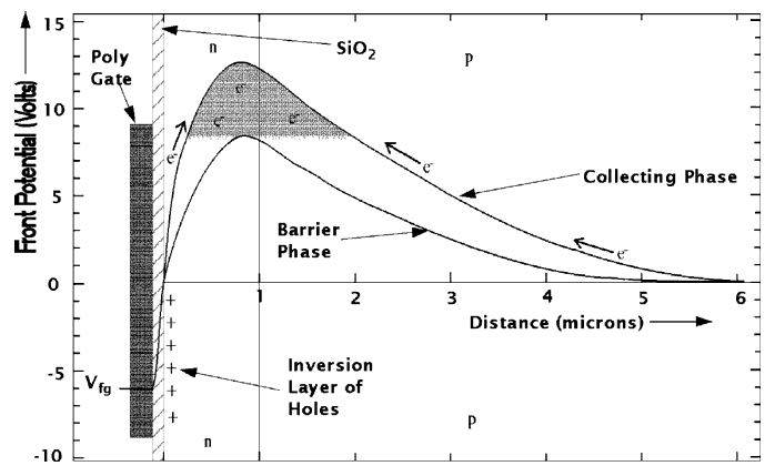
The Loral CCDs are illuminated from the 'front' surface, i.e., the light passes through the polysilicon gate structure overlying the 10µm thick active silicon layer. Because the WFPC2 devices are front-side illuminated and supported by a bulk silicon substrate, the CCD surface is flat, which has reduced the uncertainties in the astrometric calibration to about the 1/10 pixel level.
In this section the performance of the WFPC2 CCDs is reviewed, and compared to the earlier WF/PC-1 devices. A summary of device characteristics is given in Table 4.1.
| Parameter |
WF/PC-11 |
WFPC2 |
|---|---|---|
| Device |
TI |
Loral |
| Architecture |
Thinned |
Thick |
| Illumination |
back-side |
front-side |
| Format |
800×800 |
800×800 |
| Pixel size |
152 µm |
152 µm |
| UV Phosphor |
Coronene |
Lumogen |
| Dark rate |
0.03 e- pixel-1 s-1(-87°C) |
~0.0045 e- pixel-1 s-1(-88°C) |
| Read noise |
13e- RMS |
5e- RMS |
| Full well depth |
40,000 e- |
~90,000 e- |
| Gain |
8e- DN-1 |
7e- DN-1 or 14e- DN-1 |
| ADC range |
12 bits (4096 DN) |
12 bits (4096 DN) |
| Full range (e-) |
~30,000e- |
~53,000e- |
| QE 6000Å |
50% |
35% |
| QE 2500Å |
12% |
15% |
| WFC resolution |
0.10" pixel-1 |
0.0996" pixel-1 |
| PC resolution |
0.043" pixel-1 |
0.0455" pixel-1 |
| 1WF/PC-1 data are available through the STScI data archive. |
|
Space Telescope Science Institute http://www.stsci.edu Voice: (410) 338-1082 help@stsci.edu |